
In the world of FPGA-based systems, ensuring efficient and reliable program memory updates for real-time applications is crucial. As part of a project involving the BVF RiscV Subsystem on a Microchip PolarFire SoC, I faced the challenge of how to dynamically change the program memory while maintaining system integrity. Here’s how I tackled the problem.
The Need for Efficient Program Memory Management
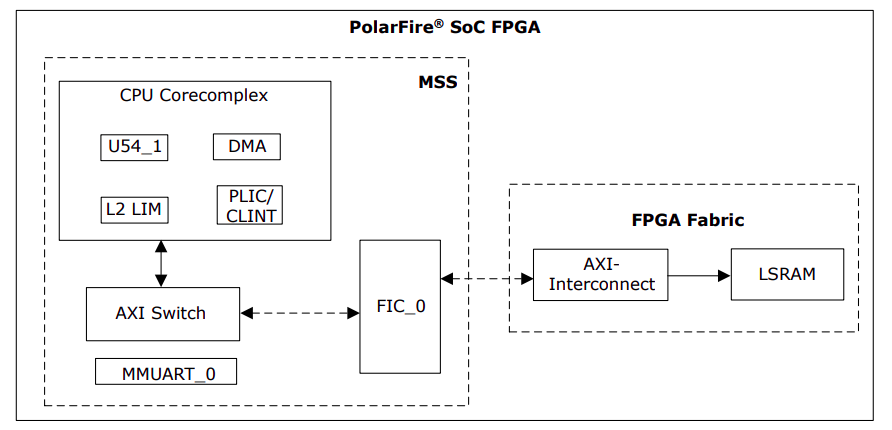
The key requirement was to establish a communication channel between the Linux system running on the BVF RiscV Subsystem and the FPGA fabric. Microchip’s Libero toolchain provides two primary communication protocols—AXI4 and APB—already configured within the system. After some exploration, I found an ideal solution in the form of Microchip’s DP (Dual Port) Memory IP block.
Leveraging Dual-Port Memory IP for Program Updates
The DP Memory IP block allows the use of FPGA LSRAMs through two distinct ports: one with a native address-data interface and another with the AXI4 protocol. This setup was perfect for my needs, enabling the AXI4 bus from the BVF RiscV Subsystem to connect to an AXI4 master-slave interconnect. By doing so, I could write data directly to the LSRAM by accessing the relevant bus location in Linux.
Microchip has predefined address ranges for its PolarFire SoC chipset, allowing access to peripherals connected to these protocol buses. By using pointers to these address ranges, it’s possible to read from or write to the associated peripheral devices. I configured the AXI DP memory interface alongside the CPU to serve as program memory, allowing the Linux system to write the program to the memory, which the Softcore CPU then accesses via the native memory interface.
Introducing APB Interface for Softcore Control
While the DP Memory IP solved the memory management issue, there was still the matter of how the Softcore CPU would be notified when a new program was written to memory. To address this, I utilized the APB interface provided by the PolarFire SoC. The APB interface facilitates reliable data transfer between the MSS and FPGA fabric in small quantities.
I developed a simple APB slave interface, using example code from the Verilog tutorial CAPE option in the Beaglev-fire gateware as a reference. The APB slave interface includes specific registers that receive or send data to and from Linux in a memory-mapped manner, similar to the AXI4 interface. These registers are crucial for monitoring and controlling the Softcore CPU.
Versatile Applications of APB Registers
Primarily, I intend to use these APB registers to:
- Reset the Softcore, allowing it to restart after flashing.
- Transfer GPIO access to the Linux system instead of the Softcore.
- Halt the Softcore without restarting it from the zeroth address.
However, the flexibility and modularity of FPGA systems mean that these registers can be repurposed for a variety of other tasks, depending on the specific needs of the project.
Conclusion
By integrating Microchip’s DP Memory IP with AXI4 and APB interfaces, I was able to create a robust solution for realtime program memory updates and Softcore CPU control. This approach not only ensures efficient memory management but also provides a versatile framework for future expansions and enhancements.
References