
After completing the on-paper implementation of the entire program memory and IO mapping for the PicoRV32 softcore, the next crucial step was to validate the low-latency performance of the system. This involved two key testing phases:
1. Testing Inline Assembly in C Programs
The first objective was to ensure that the inline assembly within a C program, which would be compiled into ELF code, operated correctly within the parameters of the PicoRV32 softcore. Inline assembly is essential for directly accessing specific CPU registers, particularly for controlling GPIOs through internal registers.
Inline assembly in C or C++ is specified using the asm or __asm__ keyword, and it follows this general form:
1
2
3
4
5
6
asm [volatile] (
    "assembly instruction"
    : output operands
    : input operands
    : clobbered registers
);
Assembly Instructions: The assembly code you want to execute. Output Operands: Values that are produced by the assembly code. Input Operands: Values that are used as inputs to the assembly code.
Clobbered Registers: Registers that are modified by the assembly code.
Clobber List: The clobber list indicates which registers (or memory) the assembly code modifies. This information is crucial for the compiler to avoid using these registers for other purposes within the same code section, preventing potential conflicts and incorrect results.
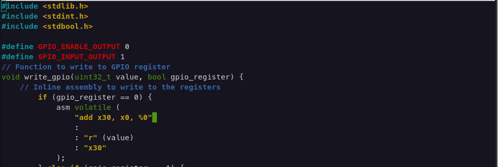
For example, in our case:
1
2
3
4
5
6
asm volatile (
    "add x30, x0, %0"
    :
    : "r" (GPIO_ENABLE_OUTPUT)
    : "x30"
);
"add x30, x0, %0": The assembly instruction to execute.- :
(empty):- No output operands. - :
"r" (GPIO_ENABLE_OUTPUT):- Specifies the input operand. Here, %0 will be replaced by GPIO_ENABLE_OUTPUT. - :
"x30": Indicates that the x30 register is modified (or clobbered) by this instruction.
By listing x30 in the clobber list, the compiler understands that the value in x30 before this instruction cannot be relied upon afterward. This helps avoid issues with register allocation and ensures that the compiler does not make assumptions about the values in x30.
2. Testing the “Flashing” of Program Memory
The second objective was to verify if the correct data is written to the FPGA LSRAM (the Program memory of the softcore) and that it is being read correctly by the hardware.
AXI4 Memory Testing
As mentioned in a previous blog post, the memory addresses are mapped for the access protocols used to communicate between the MSS (Microprocessor Subsystem) and the FPGA fabric.
For AXI4 mapping, a macro IP called FIC0 Initiator is used to connect the FPGA LSRAM through the AXI4 interconnect switch and MSS (Linux System). The FIC0 is pre-mapped to the address range 0x6000_0000 - 0x7FFF_FFFF, which has a total size of 512MB, but we will be using only 128KB out of it. While these maps are predefined within the MSS, for convenience, we will also add a device tree entry to easily recognize the device in Linux.
fabric-bus@40000000 {
    fpgalsram: uio@60000000 {
        compatible = "generic-uio";
        linux,uio-name = "fpga_lsram"; // Mandatory for program. If changed, please update program as well.
        reg = <0x0 0x60000000 0x0 0x8000>;
        status = "okay";
    };
};
Here, we define the FPGA LSRAM as a UIO device with a size of 0x8000 (hexadecimal) and a starting address of 0x6000_0000. This will allow us to simply create a pointer to the start location and start writing to the memory directly by incrementing an offset value.
APB Bus Testing
The APB bus is accessed by the FIC3-Initiator macro, and as the table suggests, it can be accessed from address 0x4000_0000. The BeagleV-Fire gateware extensively uses this protocol for various applications and has a master-to-slave interconnect IP that separates the base address to 16 different slave modules. Modules like CAPE, HSI, and M2 are some of the slave ports of this APB slave interconnect, thus we use the 12th slave port of the interconnect.
Since the base address is equally divided within all 16 slaves, we can access our CONTROL-STATUS_REGISTERS through the address 0x4C00_0000.
In our case:
1
2
localparam [7:0] REG0 = 8'h10; // READ-ONLY REGISTER at 0x4C00_0010
localparam [7:0] CONTROL_STATUS = 8'h20; // READ-WRITE REGISTER at 0x4C00_0020
Here, 0x4C is constant to access the Softcore target, while the remaining address range can be used to define as many registers as we want. All we need is an APB slave module and correct mapping on both sides.
These APB registers can be accessed in the same way as the AXI4 memory by using a pointer to the correct locations and reading or writing data at that location.
To implement this, I used a predefined C code from the Polarfire SoC lsram example by Microchip to use the memory pointers for AXI4 and made some changes to map the memory correctly. I then wrote the program data to the memory and defined a separate function to access the APB registers.
Conclusion
By conducting thorough testing of inline assembly and memory mapping, I ensured that the PicoRV32 softcore operates with the required low-latency performance. These tests were crucial in verifying the functionality of both the software and hardware components, paving the way for further development and optimization of the system.
References: